Pinmux, IO Pads, and JTAG Boundary scan
Links:
- http://www2.eng.cam.ac.uk/~dmh/4b7/resource/section14.htm
- https://www10.edacafe.com/book/ASIC/CH02/CH02.7.php
- https://ftp.libre-soc.org/Pin_Control_Subsystem_Overview.pdf
- https://bugs.libre-soc.org/show_bug.cgi?id=50
- https://bugs.libre-soc.org/show_bug.cgi?id=750
- https://bugs.libre-soc.org/show_bug.cgi?id=762
- https://git.libre-soc.org/?p=c4m-jtag.git;a=tree;hb=HEAD
- Extra info: temp pinmux info
- https://git.libre-soc.org/?p=pinmux.git;a=blob;f=src/stage2.py - Latest manual demo of pinmux generation
Managing IO on an ASIC is nowhere near as simple as on an FPGA. An FPGA has built-in IO Pads, the wires terminate inside an existing silicon block which has been tested for you. In an ASIC, you are going to have to do everything yourself. In an ASIC, a bi-directional IO Pad requires three wires (in, out, out-enable) to be routed right the way from the ASIC, all the way to the IO PAD, where only then does a wire bond connect it to a single external pin.
Below, therefore is a (simplified) diagram of what is usually contained in an FPGA's bi-directional IO Pad, and consequently this is what you must also provide, and explicitly wire up in your ASIC's HDL.

Designing an ASIC, there is no guarantee that the IO pad is working when manufactured. Worse, the peripheral could be faulty. How can you tell what the cause is? There are two possible faults, but only one symptom ("it dunt wurk"). This problem is what JTAG Boundary Scan is designed to solve. JTAG can be operated from an external digital clock, at very low frequencies (5 khz is perfectly acceptable) so there is very little risk of clock skew during that testing.
Additionally, an SoC is designed to be low cost, to use low cost packaging. ASICs are typically only 32 to 128 pins QFP in the Embedded Controller range, and between 300 to 650 FBGA in the Tablet / Smartphone range, absolute maximum of 19 mm on a side. 2 to 3 in square 1,000 pin packages common to Intel desktop processors are absolutely out of the question.
(With each pin wire bond smashing into the ASIC using purely heat of impact to melt the wire, cracks in the die can occur. The more times the bonding equipment smashes into the die, the higher the chances of irreversible damage, hence why larger pin packaged ASICs are much more expensive: not because of their manufacturing cost but because far more of them fail due to having been literally hit with a hammer many more times)
Yet, the expectation from the market is to be able to fit 1,000+ pins worth of peripherals into only 200 to 400 worth of actual IO Pads. The solution here: a GPIO Pinmux, described in some detail here https://ftp.libre-soc.org/Pin_Control_Subsystem_Overview.pdf
This page goes over the details and issues involved in creating an ASIC that combines both JTAG Boundary Scan and GPIO Muxing, down to layout considerations using coriolis2.
Resources, Platforms and Pins
When creating nmigen HDL as Modules, they typically know nothing about FPGA Boards or ASICs. They especially do not know anything about the Peripheral ICs (UART, I2C, USB, SPI, PCIe) connected to a given FPGA on a given PCB, and they should not have to.
Through the Resources, Platforms and Pins API, a level of abstraction
between peripherals, boards and HDL designs is provided. Peripherals
may be given (name, number) tuples, the HDL design may "request"
a peripheral, which is described in terms of Resources, managed
by a ResourceManager, and a Platform may provide that peripheral.
The Platform is given
the resposibility to wire up the Pins to the correct FPGA (or ASIC)
IO Pads, and it is the HDL design's responsibility to connect up
those same named Pins, on the other side, to the implementation
of the PHY/Controller, in the HDL.
Here is a function that defines a UART Resource:
#!/usr/bin/env python3
from nmigen.build.dsl import Resource, Subsignal, Pins

def UARTResource(*args, rx, tx):
  io = []
  io.append(Subsignal("rx", Pins(rx, dir="i", assert_width=1)))
  io.append(Subsignal("tx", Pins(tx, dir="o", assert_width=1)))
  return Resource.family(*args, default_name="uart", ios=io)
Note that the Subsignal is given a convenient name (tx, rx) and that there are Pins associated with it. UARTResource would typically be part of a larger function that defines, for either an FPGA or an ASIC, a full array of IO Connections:
def create_resources(pinset):
   resources = []
   resources.append(UARTResource('uart', 0, tx='A20', rx='A21'))
   # add clock and reset
   clk = Resource("clk", 0, Pins("sys_clk", dir="i"))
   rst = Resource("rst", 0, Pins("sys_rst", dir="i"))
   resources.append(clk)
   resources.append(rst)
   return resources
For an FPGA, the Pins names are typically the Ball Grid Array Pad or Pin name: A12, or N20. ASICs can do likewise: it is for convenience when referring to schematics, to use the most recogniseable well-known name.
Next, these Resources need to be handed to a ResourceManager or a Platform (Platform derives from ResourceManager)
from nmigen.build.plat import TemplatedPlatform

class ASICPlatform(TemplatedPlatform):
  def __init__(self, resources):
      super().__init__()
      self.add_resources(resources)
An HDL Module may now be created, which, if given a platform instance during elaboration, may request a UART (caveat below):
from nmigen import Elaboratable, Module, Signal

class Blinker(Elaboratable):
  def elaborate(self, platform):
      m = Module()
      # get the UART resource, mess with the output tx
      uart = platform.request('uart')
      intermediary = Signal()
      m.d.comb += uart.tx.eq(~intermediary) # invert, for fun
      m.d.comb += intermediary.eq(uart.rx) # pass rx to tx

      return m
The caveat here is that the Resources of the platform actually have to have a UART in order for it to be requestable! Thus:
resources = create_resources() # contains resource named "uart"
asic = ASICPlatform(resources)
hdl = Blinker()
asic.build(hdl)
Finally the association between HDL, Resources, and ASIC Platform is made:
- The Resources contain the abstract expression of the type of peripheral, its port names, and the corresponding names of the IO Pads associated with each port.
- The HDL which knows nothing about IO Pad names requests a Resource by name
- The ASIC Platform, given the list of Resources, takes care of connecting requests for Resources to actual IO Pads.
This is the simple version. When JTAG Boundary Scan needs to be added, it gets a lot more complex.
JTAG Boundary Scan
JTAG Scanning is a (paywalled) IEEE Standard: 1149.1 which with a little searching can be found online. Its purpose is to allow a well-defined method of testing ASIC IO pads that a Foundry or ASIC test house may apply easily with off-the-shelf equipment. Scan chaining can also connect multiple ASICs together so that the same test can be run on a large batch of ASICs at the same time.
IO Pads generally come in four primary different types:
- Input
- Output
- Output with Tristate (enable)
- Bi-directional Tristate Input/Output with direction enable
Interestingly these can all be synthesised from one Bi-directional Tristate IO Pad. Other types such as Differential Pair Transmit may also be constructed from an inverter and a pair of IO Pads. Other more advanced features include pull-up and pull-down resistors, Schmidt triggering for interrupts, different drive strengths, and so on, but the basics are that the Pad is either an input, or an output, or both.
The JTAG Boundary Scan therefore needs to know what type each pad is (In/Out/Bi) and has to "insert" itself in between all the Pad's wires, which may be just an input, or just an output, and, if bi-directional, an "output enable" line.
The "insertion" (or, "Tap") into those wires requires a pair of Muxes for each wire. Under normal operation the Muxes bypass JTAG entirely: the IO Pad is connected, through the two Muxes, directly to the Core (a hardware term for a "peripheral", in Software terminology).
When JTAG Scan is enabled, then for every pin that is "tapped into", the Muxes flip such that:
- The IO Pad is connected directly to latches controlled by the JTAG Shift Register
- The Core (peripheral) likewise but to different bits from those that the Pad is connected to
In this way, not only can JTAG control or read the IO Pad, but it can also read or control the Core (peripheral). This is its entire purpose: interception to allow for the detection and triaging of faults.
- Software may be uploaded and run which sets a bit on one of the peripheral outputs (UART Tx for example). If the UART TX IO Pad was faulty, no possibility existd without Boundary Scan to determine if the peripheral was at fault. With the UART TX pin function being redirected to a JTAG Shift Register, the results of the software setting UART Tx may be detected by checking the appropriate Shift Register bit.
- Likewise, a voltage may be applied to the UART RX Pad, and the corresponding SR bit checked to see if the pad is working. If the UART Rx peripheral was faulty this would not be possible.

C4M JTAG TAP
Staf Verhaegen's Chips4Makers JTAG TAP module includes everything needed to create JTAG Boundary Scan Shift Registers, as well as the IEEE 1149.1 Finite State Machine to access them through TMS, TDO, TDI and TCK Signalling. However, connecting up cores (a hardware term: the equivalent software term is "peripherals") on one side and the pads on the other is especially confusing, but deceptively simple. The actual addition to the Scan Shift Register is this straightforward:
from c4m.nmigen.jtag.tap import IOType, TAP

class JTAG(TAP):
   def __init__(self):
       TAP.__init__(self, ir_width=4)
       self.u_tx = self.add_io(iotype=IOType.Out, name="tx")
       self.u_rx = self.add_io(iotype=IOType.In, name="rx")
This results in the creation of:
- Two Records, one of type In named rx, the other an output named tx
- Each Record contains a pair of sub-Records: one core-side and the other pad-side
- Entries in the Boundary Scan Shift Register which if set may control (or read) either the peripheral / core or the IO PAD
- A suite of Muxes (as shown in the diagrams above) which allow either direct connection between pad and core (bypassing JTAG) or interception
During Interception Mode (Scanning) pad and core are connected to the Shift Register. During "Production" Mode, pad and core are wired directly to each other (on a per-pin basis, for every pin. Clearly this is a lot of work).
It is then your responsibility to:
- connect up each and every peripheral input and output to the right IO Core Record in your HDL
- connect up each and every IO Pad input and output to the right IO Pad in the Platform.
- This does not happen automatically and is not the responsibility of the TAP Interface, it is yours
The TAP interface connects the other side of the pads and cores Records: to the Muxes. You have to connect your side of both core and pads Records in order for the Scan to be fully functional.
Both of these tasks are painstaking and tedious in the extreme if done manually, and prone to either sheer boredom, transliteration errors, dyslexia triggering or just utter confusion. Despite this, let us proceed, and, augmenting the Blinky example, wire up a JTAG instance:
class Blinker(Elaboratable):
  def elaborate(self, platform):
      m = Module()
      m.submodules.jtag = jtag = JTAG()

      # get the records from JTAG instance
      utx, urx = jtag.u_tx, jtag.u_rx
      # get the UART resource, mess with the output tx
      p_uart = platform.request('uart')

      # uart core-side from JTAG
      intermediary = Signal()
      m.d.comb += utx.core.o.eq(~intermediary) # invert, for fun
      m.d.comb += intermediary.eq(urx.core.i) # pass rx to tx

      # wire up the IO Pads (in right direction) to Platform
      m.d.comb += uart.rx.eq(utx.pad.i) # receive rx from JTAG input pad
      m.d.comb += utx.pad.o.eq(uart.tx) # transmit tx to JTAG output pad
      return m
Compared to the non-scan-capable version, which connected UART Core Tx and Rx directly to the Platform Resource (and the Platform took care of wiring to IO Pads):
- Core HDL is instead wired to the core-side of JTAG Scan
- JTAG Pad side is instead wired to the Platform
- (the Platform still takes care of wiring to actual IO Pads)
JTAG TAP capability on UART TX and RX has now been inserted into the chain. Using openocd or other program it is possible to send TDI, TMS, TDO and TCK signals according to IEEE 1149.1 in order to intercept both the core and IO Pads, both input and output, and confirm the correct functionality of one even if the other is broken, during ASIC testing.
Libre-SOC Automatic Boundary Scan
Libre-SOC's JTAG TAP Boundary Scan system is a little more sophisticated: it hooks into (replaces) ResourceManager.request(), intercepting the request and recording what was requested. The above manual linkup to JTAG TAP is then taken care of automatically and transparently, but to all intents and purposes looking exactly like a Platform even to the extent of taking the exact same list of Resources.
class Blinker(Elaboratable):
  def __init__(self, resources):
      self.jtag = JTAG(resources)

  def elaborate(self, platform):
      m = Module()
      m.submodules.jtag = jtag = self.jtag

      # get the UART resource, mess with the output tx
      uart = jtag.request('uart')
      intermediary = Signal()
      m.d.comb += uart.tx.eq(~intermediary) # invert, for fun
      m.d.comb += intermediary.eq(uart.rx) # pass rx to tx

      return jtag.boundary_elaborate(m, platform)
Connecting up and building the ASIC is as simple as a non-JTAG, non-scanning-aware Platform:
resources = create_resources()
asic = ASICPlatform(resources)
hdl = Blinker(resources)
asic.build(hdl)
The differences:
- The list of resources was also passed to the HDL Module such that JTAG may create a complete identical list of both core and pad matching Pins
- Resources were requested from the JTAG instance, not the Platform
- A "magic function" (JTAG.boundary_elaborate) is called which wires up all of the seamlessly intercepted Platform resources to the JTAG core/pads Resources, where the HDL connected to the core side, exactly as if this was a non-JTAG-Scan-aware Platform.
- ASICPlatform still takes care of connecting to actual IO Pads, except that the Platform.resource requests were triggered "behind the scenes". For that to work it is absolutely essential that the JTAG instance and the ASICPlatform be given the exact same list of Resources.
Clock synchronisation
Take for example USB ULPI:
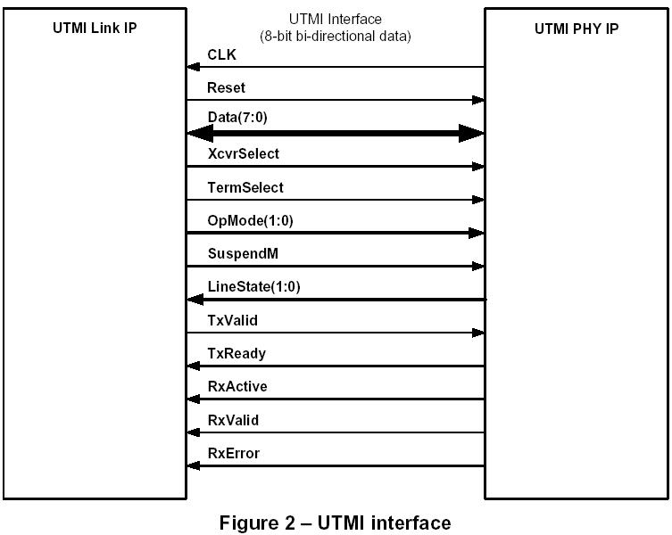
Here there is an external incoming clock, generated by the PHY, to which both Received and Transmitted data and control is synchronised. Notice very specifically that it is not the main processor generating that clock Signal, but the external peripheral (known as a PHY in Hardware terminology)
Firstly: note that the Clock will, obviously, also need to be routed through JTAG Boundary Scan, because, after all, it is being received through just another ordinary IO Pad, after all. Secondly: note that if it didn't, then clock skew would occur for that peripheral because although the Data Wires went through JTAG Boundary Scan MUXes, the clock did not. Clearly this would be a problem.
However, clocks are very special signals: they have to be distributed evenly to all and any Latches (DFFs) inside the peripheral so that data corruption does not occur because of tiny delays. To avoid that scenario, Clock Domain Crossing (CDC) is used, with Asynchronous FIFOs:
    rx_fifo = stream.AsyncFIFO([("data", 8)], self.rx_depth, w_domain="ulpi", r_domain="sync")
    tx_fifo = stream.AsyncFIFO([("data", 8)], self.tx_depth, w_domain="sync", r_domain="ulpi")
    m.submodules.rx_fifo = rx_fifo
    m.submodules.tx_fifo = tx_fifo
However the entire FIFO must be covered by two Clock H-Trees: one by the ULPI external clock, and the other the main system clock. The size of the ULPI clock H-Tree, and consequently the size of the PHY on-chip, will result in more Clock Tree Buffers being inserted into the chain, and, correspondingly, matching buffers on the ULPI data input side likewise must be inserted so that the input data timing precisely matches that of its clock.
The problem is not receiving of data, though: it is transmission on the output ULPI side. With the ULPI Clock Tree having buffers inserted, each buffer creates delay. The ULPI output FIFO has to correspondingly be synchronised not to the original incoming clock but to that clock after going through H Tree Buffers. Therefore, there will be a lag on the output data compared to the incoming (external) clock
Pinmux GPIO Block
The following diagram is an example of a mux'd GPIO block that comes from the Ericson presentation on a GPIO architecture.

Our Pinmux Block
The block we are developing is very similar, but is lacking some of configuration of the former (due to complexity and time constraints).
The implemented pinmux uses two sub-blocks:
A Wishbone controlled N-GPIO block.
N-port I/O multiplexer (for current usecase set to 4 ports).
Terminology
For clearer explanation, the following definitions will be used in the text. As the documentation is actively being written, the experimental code may not adhere to these all the time.
- Bank - A group of contiguous pins under a common name.
- Pin - Bi-directional wire connecting to the chip's pads.
- Function (pin) - A signal used by the peripheral.
- Port - Bi-directional signal on the peripheral and pad sides of the multiplexer.
- Muxwidth - Number of input ports to the multiplexers
- PinMux - Multiplexer for connecting multiple peripheral functions to one IO pad.
For example:
A 128-pin chip has 4 banks N/S/E/W corresponding to the 4 sides of the chip. Each bank has 32 pins. Each pin can have up to 4 multiplexed functions, thus the multiplexer width for each pin is 4.
PinSpec Class
- https://git.libre-soc.org/?p=pinmux.git;a=blob;f=src/spec/base.py;h=c8fa2b09d650b1b7cfdb499bfe711a3ebaf5848b;hb=HEAD PinSpec class defined here.
PinSpec is a powerful construct designed to hold all the necessary information about the chip's banks. This includes:
- Number of banks
- Number of pins per each bank
- Peripherals present (UART, GPIO, I2C, etc.)
- Mux configuration for every pin (mux0: gpio, mux1: uart tx, etc.)
- Peripheral function signal type (out/in/bi)
Pinouts
- https://git.libre-soc.org/?p=pinmux.git;a=blob;f=src/spec/interfaces.py;h=f5ecf4817ba439b607a1909a4fcb6aa2589e2afd;hb=HEAD Pinouts class defined here.
The Pinspec class inherits from the Pinouts class, which allows to view the dictionaries containing bank names and pin information.
- keys() - returns dict_key object of all the pins (summing all the banks) which is iterable
- items() - a dict_key of pins, with each pin's mux information
For example, PinSpec object 'ps' has one bank 'A' with 4 pins ps.keys() returns dict_keys([0, 1, 2, 3]) ps.items() returns dict_items([(0, {0: ('GPIOA_A0', 'A'), 1: ('UART0_TX', 'A'), 2: ('TWI0_SDA', 'A')}), (1, {0: ('GPIOA_A1', 'A'), 1: ('UART0_RX', 'A'), 2: ('TWI0_SCL', 'A')}), (2, {0: ('GPIOA_A2', 'A')}), (3, {0: ('GPIOA_A3', 'A')})])
PinGen
pinfunctions.py contains the "pinspec" list containing the Python functions which generate the necessary signals for gpio, uart, i2c, etc. (with IOType information). PinGen class uses "call" and "pinspec" to effectively create a Lambda function for generating specified peripheral signals.
The GPIO block
NOTE ! - Need to change 'bank' terminology for the GPIO block in doc and code!

The GPIO module is multi-GPIO block integral to the pinmux system. To make the block flexible, it has a variable number of of I/Os based on an input parameter.
Configuration Word
After a discussion with Luke on IRC (14th January 2022), new layout of the 8-bit data word for configuring the GPIO (through WB):
- oe - Output Enable (see the Ericson presentation for the GPIO diagram)
- ie - Input Enable (Not used, as IOPad only supports i/o/oe)
- puen - Pull-Up resistor enable
- pden - Pull-Down resistor enable
- i/o - When configured as output (oe set), this bit sets/clears output. When configured as input, shows the current state of input (read-only)
- bank[2:0] - Bank Select (only 4 banks used, bank[2] used for JTAG chain)
Simultaneous/Packed Configuration
To make the configuration more efficient, multiple GPIOs can be configured with one data word. The number of GPIOs in one "row" is dependent on the WB data bus width and granuality (see Wishbone B4 spec, section 3.5 Data Organization for more details).
If for example, the data bus is 64-bits wide and granuality is 8, eight GPIO configuration bytes - and thus eight GPIOs - can be configured in one go. To configure only certain GPIOs, the WB sel signal can be used (see next section).
(NOTE: Currently the code doesn't support granuality higher than 8)
The diagram below shows the layout of the configuration byte.

If the block is created with more GPIOs than can fit in a single data word, the next set of GPIOs can be accessed by incrementing the address. For example, if 16 GPIOs are instantiated and 64-bit data bus is used, GPIOs 0-7 are accessed via address 0, whereas GPIOs 8-15 are accessed by address 1.
Example Memory Map
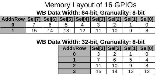
The diagrams above show the difference in memory layout between 16-GPIO block implemented with 64-bit and 32-bit WB data buses. The 64-bit case shows there are two rows with eight GPIOs in each, and it will take two writes (assuming simple WB write) to completely configure all 16 GPIOs. The 32-bit on the other hand has four address rows, and so will take four write transactions.
64-bit:
- 0x00 - Configure GPIOs 0-7 - requires 8-bit
selone bit per GPIO - 0x01 - Configure GPIOs 8-15 - requires 8-bit
selone bit per GPIO
32-bit:
- 0x00 - Configure GPIOs 0-3 - requires 4-bit
selone bit per GPIO - 0x01 - Configure GPIOs 4-7 - requires 4-bit
selone bit per GPIO - 0x02 - Configure GPIOs 8-11 - requires 4-bit
selone bit per GPIO - 0x03 - Configure GPIOs 12-15 - requires 4-bit
selone bit per GPIO
Here is the pseudocode for reading the GPIO data structs:
read_bytes = []
for i in range(len(sel)):
    GPIO_num = adr*len(sel)+i
    if sel[i]:
        read_bytes.append(GPIO[GPIO_num])
    else:
        read_bytes.append(Const(0, 8))
if not wen:
    dat_r.eq(Cat(read_bytes))
and for writing, slightly different style:
if wen:
    write_bytes = []
    for i in range(len(sel)):
        GPIO_num = adr*len(sel)+i
        write_byte = dat_w.bit_select(i*8, 8)
        if sel[i]:
            GPIO[GPIO_num].eq(write_byte)
As explained in this video https://m.youtube.com/watch?v=Pf6gmDQnw_4
if each GPIO is mapped to one single byte, and it is assumed that
the sel lines are enough to always give byte-level read/write
then the GPIO number becomes the Memory-mapped byte number, hence
the use of len(sel) above. len(dat_r)//8 would do as well
because these should be equal.
The IO Mux block

This block is an N-to-1 (4-port shown above) mux and it simultaneously connects:
o/oe signals from one of N peripheral ports, to the pad output port
i pad port signal to one of N peripheral ports (the rest being set to 0).
The block is then used in a higher-level pinmux block, and instantiated for each pin.
Combined Block
NOTE ! - Need to change 'bank' terminology for the GPIO block in doc and code!

The GPIO and IOMux blocks are combined in a single block called the Pinmux block.
By default, bank 0 is hard-wired to the memory-mapped WB bus GPIO. The CPU core can just write the configuration word to the GPIO row address. From this perspective, it is no different to a conventional GPIO block.
Bank select, allows to switch over the control of the IO pad to another peripheral. The peripheral will be given sole connectivity to the o/oe/i signals, while additional parameters such as pull up/down will either be automatically configured (as the case for I2C), or will be configurable via the WB bus. (This has not been implemented yet, so open to discussion)
Bank Select Options
- bank 0 - WB bus has full control (GPIO peripheral)
- bank 1,2,3 - WB bus only controls puen/pden, periphal gets o/oe/i (whether ie should be routed out is not finalised yet)
Adding JTAG BS Chain to the Pinmux block (In Progress)
The JTAG BS chain need to have access to the bank select bits, to allow selecting different peripherals during testing. At the same time, JTAG may also require access to the WB bus to access GPIO configuration options not available to bank 1/2/3 peripherals.
The proposed JTAG BS chain is as follows:
- Connect puen/pden/bank from GPIO block to the IOMux through JTAG BS chain.
- Connect the i/o/oe pad port from IOMux via JTAG BS chain.
 Test port for configuring GPIO without WB? - utilising bank bit 2?
- Way to drive WB via JTAG?
Such a setup would allow the JTAG chain to control the bank select when testing connectivity of the peripherals, as well as give full control to the GPIO configuration when bank select bit 2 is set.
For the purposes of muxing peripherals, bank select bit 2 is ignored. This means that even if JTAG is handed over full control, the peripheral is still connected to the GPIO block (via the BS chain).
Signals for various ports:
- WB bus or Periph0: WB data read, data write, address, sel, cyc, stb, ack
- Periph1/2/3: o,oe,i (puen/pden are only controlled by WB, test port, or fixed by functionality; ie not used yet)
- Test port: bank[2:0], o,oe,i,ie,puen,pden. In addition, internal
address to access individual GPIOs will be available (this will consist of a
few bits, as more than 16 GPIOs per block is likely to be to big).
As you can see by the above list, the pinmux block is becoming quite a complex beast. If there are suggestions to simplify or reduce some of the signals, that will be helpful.
The diagrams above showed 1-bit GPIO connectivity. Below you'll find the 4-bit case (NOT IMPLEMENTED YET).
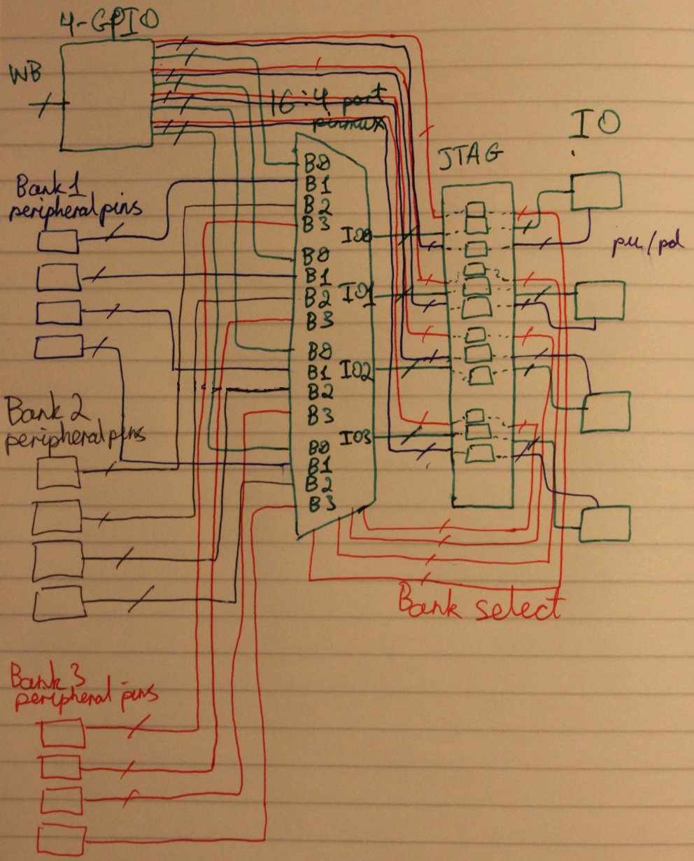
Core/Pad Connection + JTAG Mux
Diagram constructed from the nmigen plat.py file.
