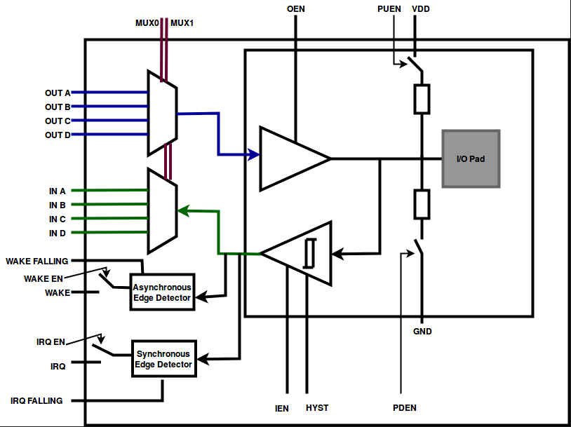
Pin Multiplexing
- http://bugs.libre-riscv.org/show_bug.cgi?id=8
- https://github.com/sifive/sifive-blocks/tree/master/src/main/scala/devices/ includes GPIO, SPI, UART, JTAG, I2C, PinCtrl, UART and PWM. Also included is a Watchdog Timer and others.
- https://github.com/sifive/freedom/blob/master/src/main/scala/everywhere/e300artydevkit/Platform.scala Pinmux ("IOF") for multiplexing several I/O functions onto a single pin
- https://bitbucket.org/casl/pinmux.git - implementation by Shakti RISE Group
Surprisingly complex!
Requirements
"to create a general-purpose libre-licensed pinmux module that can be used with a wide range of interfaces that have Open-Drain, Push-Pull and bi-directional capabilities, as well as optional pull-up and pull-down resistors, in an IDENTICAL fashion to that of ALL major well-known embedded SoCs from ST Micro, Cypress, Texas Instruments, NXP, Rockchip, Allwinner and many many others".
- The IO pad shall have pull-up enable, pull-down enable, variable frequency de-bounce (schmidt trigger), tri-state capability, variable current drive (on input), Open Drain and CMOS Push-Pull.
- Certain functions shall have the ability to control whether IO pads will be input or output (not the GPIO registers).
- Number of wires shall be minimised especially in cases where the IO pad (puen, oe) need to change under the control of the function (not the GPIO registers).
- The amount of latency (gates in between I/O pad and function) shall be minimised
- There shall be no short-circuits created by multiple input pins trying to drive the same input function
- There shall be no short-circuits even when functions control when the IO pad is an input.
Analysis
Questions:
- Can damage occur (to the ASIC) by outputs being short-circuited to outputs in any way? A partial analysis showed that because outputs are one-to-many, there should not be a possibility for that to occur. However what if a function is bi-directional?
- Is de-bouncing always needed on every input? Is it ok for de-bouncing to be only done on EINT?
- Can the input mux be turned round and "selector" logic added so that there is no possibility of damage to inputs?
Images
GSoC2018
Introductions:
- Luke Kenneth Casson Leighton (lkcl) - reverse-engineer, software libre advocate, assembly-level programming and disassembly, python, c, c++, gate-level circuit and ASIC design, PCB design and assembly, 3D CAD design, lots of different stuff. Guardian of the EOMA68 Certification Mark, and currently responsible for coordinating the design of a fully Libre RISC-V SoC in collaboration with the RISE Group, IIT Madras, Shakti Project. not much experience at verilog (have done a couple of tutorials).
- Aurojyoti Das(auro) - graduate student (MSc Electrical - Microelectronics) at TU Delft, Netherlands. C/C++, Verilog, VHDL, SystemVerilog, RTL Design, Logic Verification, Python/Perl/Shell scripting, Analog IC Design (currently learning)
Hardware available:
- lkcl: ZC706
- xing: zynq-7020 and Xilinx XC7A100T-484 if needed contact him! higuoxing@gmail.com
Discussion and Links
- https://elinux.org/images/b/b6/Pin_Control_Subsystem_Overview.pdf
- https://lists.librecores.org/pipermail/discussion/2018-February/thread.html
- https://lists.librecores.org/pipermail/discussion/2018-January/000404.html
Some Useful Resource
- https://github.com/ucb-bar/generator-bootcamp Interactive tutorial on Scala and Chisel (best one, take it, trust me!)
- https://docs.scala-lang.org/tour/tour-of-scala.html A brief Scala tutorial
- https://github.com/ucb-bar/chisel-tutorial A brief Chisel tutorial
- https://github.com/xfguo/tbgen/blob/master/tbgen.py auto-generated test module for verilog
- https://github.com/kdurant/verilog-testbench described here https://www.vim.org/scripts/script.php?script_id=4596
- http://agilesoc.com/open-source-projects/svunit/ - SVunit - unit testing for verilog
- FPGA Overview Useful in writing GPIO related codes...
Pinouts Specification
Covered in pinouts. The general idea is to target several distinct applications and, by trial-and-error, create a pinmux table that successfully covers all the target scenarios by providing absolutely all required functions for each and every target. A few general rules:
- Different functions (SPI, I2C) which overlap on the same pins on one bank should also be duplicated on completely different banks, both from each other and also the bank on which they overlap. With each bank having separate Power Domains this strategy increases the chances of being able to place low-power and high-power peripherals and sensors on separate GPIO banks without needing external level-shifters.
- Functions which have optional bus-widths (eMMC: 1/2/4/8) may have more functions overlapping them than would otherwise normally be considered.
- Then the same overlapped high-order bus pins can also be mapped onto other pins. This particularly applies to the very large buses, such as FlexBus (over 50 pins). However if the overlapped pins are on a different bank it becomes necessary to have both banks run in the same GPIO Power Domain.
- All functions should really be pin-muxed at least twice, preferably three times. Four or more times on average makes it pointless to even have four-way pinmuxing at all, so this should be avoided. The only exceptions (functions which have not been pinmuxed multiple times) are the RGB/TTL LCD channel, and both ULPI interfaces.
GPIO Pinmux Power Domains
Of particular importance is the Power Domains for the GPIO. Realistically it has to be flexible (simplest option: recommended to be between 1.8v and 3.3v) as the majority of low-cost mass-produced sensors and peripherals on I2C, SPI, UART and SD/MMC are at or are compatible with this voltage range. Long-tail (older / stable / low-cost / mass-produced) peripherals in particular tend to be 3.3v, whereas newer ones with a particular focus on Mobile tend to be 1.2v to 1.8v.
A large percentage of sensors and peripherals have separate IO voltage domains from their main supply voltage: a good example is the SN75LVDS83b which has one power domain for the RGB/TTL I/O, one for the LVDS output, and one for the internal logic controller (typical deployments tend not to notice the different power-domain capability, as they usually supply all three voltages at 3.3v).
Relying on this capability, however, by selecting a fixed voltage for the entire SoC's GPIO domain, is simply not a good idea: all sensors and peripherals which do not have a variable (VREF) capability for the logic side, or coincidentally are not at the exact same fixed voltage, will simply not be compatible if they are high-speed CMOS-level push-pull driven. Open-Drain on the other hand can be handled with a MOSFET for two-way or even a diode for one-way depending on the levels, but this means significant numbers of external components if the number of lines is large.
So, selecting a fixed voltage (such as 1.8v or 3.3v) results in a bit of a problem: external level-shifting is required on pretty much absolutely every single pin, particularly the high-speed (CMOS) push-pull I/O. An example: the DM9000 is best run at 3.3v. A fixed 1.8v FlexBus would require a whopping 18 pins (possibly even 24 for a 16-bit-wide bus) worth of level-shifting, which is not just costly but also a huge amount of PCB space: bear in mind that for level-shifting, an IC with double the number of pins being level-shifted is required.
Given that level-shifting is an unavoidable necessity, and external level-shifting has such high cost(s), the workable solution is to actually include GPIO-group level-shifting actually on the SoC die, after the pin-muxer at the front-end (on the I/O pads of the die), on a per-bank basis. This is an extremely common technique that is deployed across a very wide range of mass-volume SoCs.
One very useful side-effect for example of a variable Power Domain voltage on a GPIO bank containing SD/MMC functionality is to be able to change the bank's voltage from 3.3v to 1.8v, to match an SD Card's capabilities, as permitted under the SD/MMC Specification. The alternative is to be forced to deploy an external level-shifter IC (if PCB space and BOM target allows) or to fix the voltage at 3.3v and thus lose access to the low-power and higher-speed capabilities of modern SD Cards.
In summary: putting level shifters right at the I/O pads of the SoC, after the pin-mux (so that the core logic remains at the core voltage) is a cost-effective solution that can have additional unintended side-benefits and cost savings beyond simply saving on external level-shifting components and board space.